In this project, it is aimed to design and implement a VGA and UART controller for an FPGA-based game console. The system is implemented on an Artix-7 FPGA on a Basys3 board. It utilizes available peripherals and follows a hierarchical design to enable modular integration.
The system consists of:
- Peripheral modules handling video signal generation, UART communication, buttons, switches, LEDs, seven-segment displays, and peripheral debouncing
- Internal service modules handling clock division, reset generation, renderers, pseudo-random number generation for maps
- Game logic modules handling player movement and collision detection, map generation, game state management and score tracking, and difficulty scaling.
VGA Driver and Video Signal Generation
VGA operates by raster scanning: an electron beam (or digital equivalent) sweeps left-to-right across each horizontal line, then moves down to the next line, repeating until the full frame is drawn. Two synchronization signals (hsync and vsync) control this scanning process.
While the technology evolved from CRTs, the timing requirements remain with today’s digital displays. To accommodate the movement of the beam in the CRT displays, several sync delays are baked into how VGA works. To drive a 640x480 display at 60Hz, two counters of lengths 800 and 525 are used, which are active-low for 96 and 2 cycles respectively to generate the hsync and vsync signals. The active video signal is generated when both counters are within the visible area of the display, which is 640 pixels for horizontal and 480 lines for vertical.
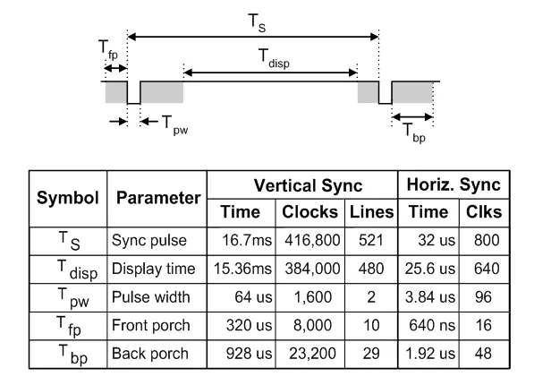
Simple counters are used to generate the sync signals and pixel output. At the end of each horizontal scan, the vertical counter is incremented and these counters are fed to the signal generation logic.
The active-low 96 clock cycles hsync and 2 clock cycles vsync signals are generated right after the visible area of the display and the front porch duration, which is the time it takes for the beam to move from the end of the visible area to the start of the sync pulse in CRT displays.
assign hsync = ~((h_counter >= (H_VISIBLE + H_FP)) && (h_counter < (H_VISIBLE + H_FP + H_SYNC)));
assign vsync = ~((v_counter >= (V_VISIBLE + V_FP)) && (v_counter < (V_VISIBLE + V_FP + V_SYNC)));
Following the sync pulse, the back porch duration is accounted for in the timing. The back porch is the time it takes for the beam to move from the end of the sync pulse to the start of the visible area. During back and front porch, a blank signal is sent to ensure no visual artifacts are introduced during transitions in VGA signal generation. For a 25 MHz pixel clock in this design, the refresh rate is 59.52 Hz, ~0.7% of the VESA Standard 59.94 Hz.
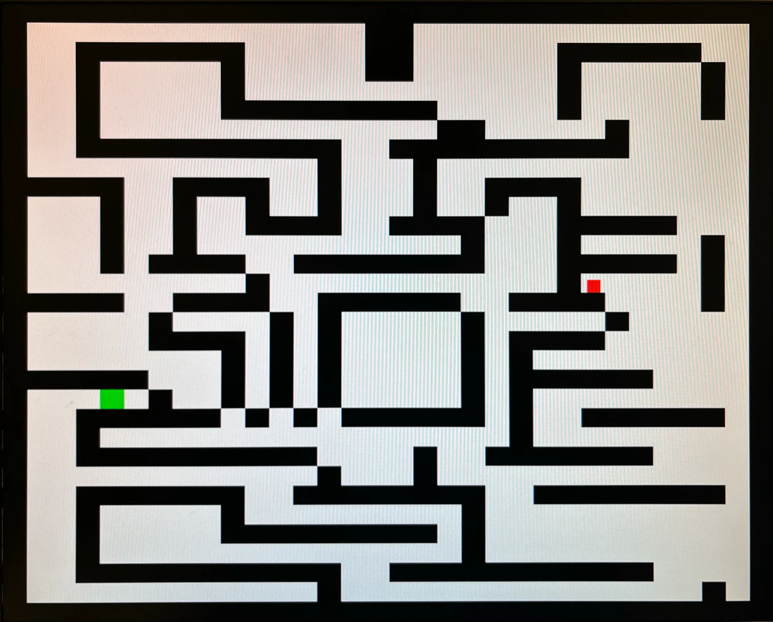
The visible pixel and whether the signal is in the visible range is outputted by the module, to be used by the rendering engine. The rendering engine generates the pixel data based on the game state and outputs it synchronously from the VGA ports. The display then locks into the hsync and vsync pulses to render the data coming from color channel ports at the timed pixel.
always @(*) begin
    if (!display_on) begin
        red = 0; // transmit RGB 0 to avoid visual artifacts
        ...
    else begin
        if (cell_x == goal_x_i && cell_y == goal_y_i) begin // game related logic
            if (player_here && player_pixel) begin
                red = 4'hF; green = 4'd0; blue = 4'd0;
                ...
end

assign vgaRed_o   = red;
...
UART Controller
A byte of data can be received serially over a dedicated line of the FPGA using the UART protocol, allowing communication with a host computer. The transmission follows a simple protocol where an active-low start signal is sent on a pull-up line, followed by a sequence of bits with respect to the symbol rate and a single active-high stop bit at the end.
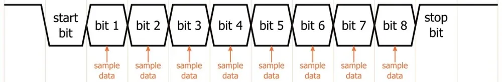
To handle the parsing, a simple state machine, a shift register, and a clock counter is used. The state machine starts in an idle state. When the line is pulled down, it counts up to half a symbol period to detect a valid start bit. If the start bit is valid, it samples the line at the symbol rate and shifts the data bits into a register sequentially. Once all 8 bits are received, it waits for the stop bit and then outputs the received byte along with a valid signal. In this design, the UART module operates with a 100 MHz clock and a symbol rate of 9600 baud.
Random Map Generation and Game Logic
The game logic includes LFSR-based pseudo-random number generation for map creation. For each generation, the player and the goal are placed on separate random cells. The difficulty scaling adjusts the size of the map and the distance between the player and the goal. A simple collision detection keeps the player within the bounds and the obstacles in the map. The player is allowed to break through a limited number of walls at the cost of points. Higher difficulty levels yield more points upon completion.
Peripherals
The system also includes modules for handling buttons, switches, LEDs, seven-segment displays, and peripheral debouncing. The buttons are used for player movement and game interactions, while the switches can be used to select predefined maps, set difficulty or switch to UART control. The LEDs provide visual feedback for game states, and the seven-segment displays show the score. The debouncing module ensures that button presses are registered accurately without multiple triggers from a single press.
Performance Metrics and Resource Utilization
Post-implementation resource utilization for the design is given below.
| Resource | Utilization | Available | Utilization % |
|---|---|---|---|
| LUT | 6563 | 20800 | 31.03 |
| LUTRAM | 432 | 9600 | 4.5 |
| FF | 11381 | 41600 | 27.36 |
| BRAM | 1.5 | 50 | 3 |
| IO | 61 | 106 | 57.55 |
| BUFG | 8 | 32 | 25 |
| MMCM | 1 | 5 | 20 |
A moderate look-up-table utilization is observed from the combinational logic in the peripherals and game logic modules. The flip-flop utilization is also significant, primarily due to the state machines and registers used for game state management and UART communication, however, allows headroom for expansion. The IO utilization is relatively high, which is expected given the number of peripherals used in the design. Overall, the resource utilization is within acceptable limits for the target FPGA, allowing for potential future expansions or optimizations in the design. Worst Negative Slack (WNS) is +0.305 ns, indicating that the design meets timing at 100 MHz with 0.305 ns margin.